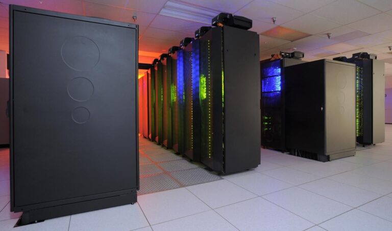
Image: Aileen Devlin/Jefferson Lab from Newport News, USA · Public domain · Wikimedia Commons
Shared multi-project wafer runs that let a small team prototype silicon photonics chips.
What it changes
Turns a full wafer tape-out into a shared run with a public entry route, so a startup can fabricate real photonic chips instead of simulating forever.
Availability
Generally available (us)
Access and cost
Get AIM Photonics MPW — Runs are priced per PIC type with customization options; a design review and quote come before a shuttle booking.
Evidence it works
- Runs silicon photonics prototyping on 300 mm wafers at the Albany NanoTech complex with test and packaging in Rochester. — source
- Offers several PIC types, including base active and low-loss active silicon photonic wafers, each with customization options. — source
What it cannot do yet
- Runs share a wafer with other projects, so the process stack and schedule are set by the shuttle, not by the customer.
- Prototyping leads to prototypes: volume production still moves to a commercial foundry.
AIM Photonics · Hardware · Last verified 2026-09-17. Claims are re-checked on a 30-day clock; the date above is when this line was last confirmed.
About the Author